CH32V003
Choose a part · Pin viewer · Pin maps · Examples · Documents · Address map
Quick start
Programming and debug: 1-wire SDI (WCH-Link, Serial Debug Interface).
Debug / serial defaults
Where these land without writing a remap register. SWD is live at reset; the UART pads are not – the pin must still be put into alternate-function mode. See route in evidence/README.ja.md.
| Series | SWDIO | SWCLK | UART TX | UART RX |
|---|---|---|---|---|
| CH32V003 | PD1 | - | PD5 (USART1) | PD6 (USART1) |
Series
| Series | Core | ISA | Flash | SRAM | Main clock | VDD | Packages | Products | Official |
|---|---|---|---|---|---|---|---|---|---|
| CH32V003 | QingKe V2A | RV32EC | 16K | 2K | 48 MHz | 2.7-5.5V | QFN20,SOP16,SOP8,TSSOP20 | 4 | en / zh |
Product comparison
CH32V003 product comparison
Only the 3 rows that differ between these 4 products; the other 9 are the same for all of them.
| CH32V003A4M6(SOP16) | CH32V003F4P6(TSSOP20) | CH32V003F4U6(QFN20) | CH32V003J4M6(SOP8) | |
|---|---|---|---|---|
| GPIO | 14 | 18 | 18 | 6 |
| ADC Channel No. | 6 | 8 | 8 | 6 |
| SPI | - | 1 | 1 | - |
All 12 rows
| | [CH32V003A4M6](https://ch32-riscv-ug.github.io/ch32-device-data/pins.html?chip=CH32V003A4M6)(SOP16) | [CH32V003F4P6](https://ch32-riscv-ug.github.io/ch32-device-data/pins.html?chip=CH32V003F4P6)(TSSOP20) | [CH32V003F4U6](https://ch32-riscv-ug.github.io/ch32-device-data/pins.html?chip=CH32V003F4U6)(QFN20) | [CH32V003J4M6](https://ch32-riscv-ug.github.io/ch32-device-data/pins.html?chip=CH32V003J4M6)(SOP8) | |---|---|---|---|---| | **Flash** | 16K | 16K | 16K | 16K | | **SRAM** | 2K | 2K | 2K | 2K | | **GPIO** | 14 | 18 | 18 | 6 | | **Temperature** | -40..85C | -40..85C | -40..85C | -40..85C | | Advanced-control timer | 1 | 1 | 1 | 1 | | General-purpose timer | 1 | 1 | 1 | 1 | | Watchdog | 2 | 2 | 2 | 2 | | System clock source | 3 | 3 | 3 | 3 | | ADC Channel No. | 6 | 8 | 8 | 6 | | I2C | 1 | 1 | 1 | 1 | | SPI | - | 1 | 1 | - | | USART | 1 | 1 | 1 | 1 |Packages & pinout drawings
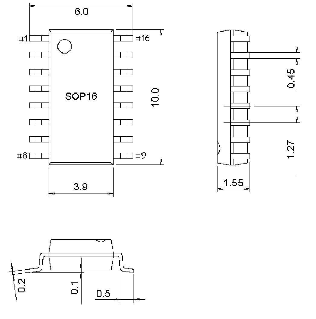
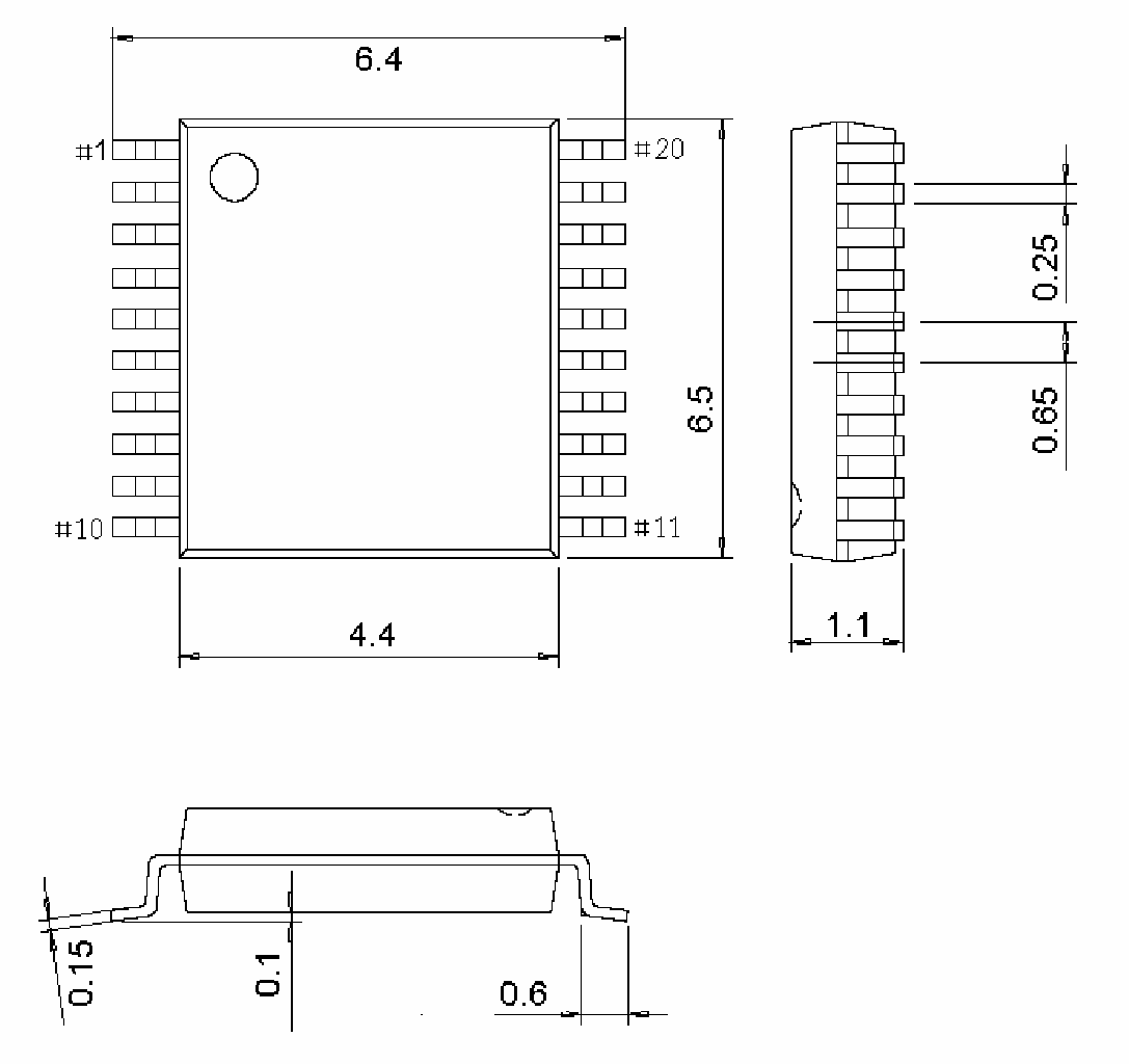
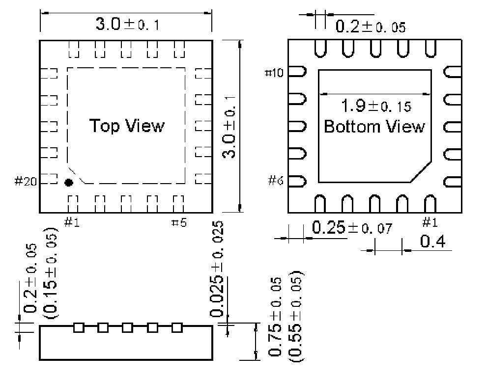
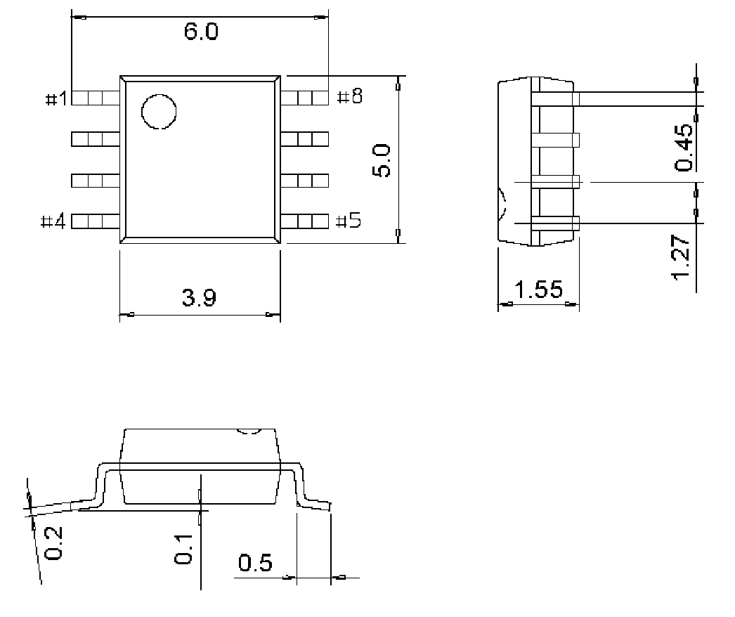
Pinout drawings are in the datasheet (chapter Pinouts):
| Package | Products | Datasheet | Outline |
|---|---|---|---|
| SOP16 | CH32V003A4M6 | en / zh | drawing |
| TSSOP20 | CH32V003F4P6 | en / zh | drawing |
| QFN20 | CH32V003F4U6 | en / zh | drawing |
| SOP8 | CH32V003J4M6 | en / zh | drawing |
Pin maps & alternate functions
[!NOTE] These are the pin-table superset: the datasheet prints one pad table for every product that shares a pinout, so a pad row does not mean this part has the peripheral. Use the product comparison table above for what a given part number contains.
CH32V003 pin map
Pin functions (filterable): ALL ADC I2C SPI SYS TIM UART USB
| Pin name | Type | CH32V003A4M6(SOP16) | CH32V003F4P6(TSSOP20) | CH32V003F4U6(QFN20) | CH32V003J4M6(SOP8) | Notes |
|---|---|---|---|---|---|---|
| PA1 | I/O/A | 12 | 5 | 2 | 1 | OSC |
| PA2 | I/O/A | 13 | 6 | 3 | 3 | OSC |
| PC0 | I/O | 16 | 10 | 7 | - | |
| PC1 | I/O/FT | 1 | 11 | 8 | 5 | |
| PC2 | I/O/FT | 2 | 12 | 9 | 6 | |
| PC3 | I/O | 3 | 13 | 10 | - | |
| PC4 | I/O/A | 4 | 14 | 11 | 7 | |
| PC5 | I/O/FT | - | 15 | 12 | - | |
| PC6 | I/O/FT | 5 | 16 | 13 | - | |
| PC7 | I/O | 6 | 17 | 14 | - | |
| PD0 | I/O/A | - | 8 | 5 | - | |
| PD1 | I/O/A | 7 | 18 | 15 | 8 | SWDIO |
| PD2 | I/O/A | - | 19 | 16 | - | |
| PD3 | I/O/A | - | 20 | 17 | - | |
| PD4 | I/O/A | 8 | 1 | 18 | 8 | |
| PD5 | I/O/A | 9 | 2 | 19 | 8 | UART TX (USART1) |
| PD6 | I/O/A | 10 | 3 | 20 | 1 | UART RX (USART1) |
| PD7 | I/O/A | 11 | 4 | 1 | - | |
| VDD | P | 15 | 9 | 6 | 4 | |
| VSS | P | 14 | 7 | 4/EP | 2 |
CH32V003 alternate functions
| Pad | default | (no route stated) | remap-1 | remap-2 | remap-3 | |---|---|---|---|---|---| | PA1 | A1, OPN0, T1CH2 | OSCI | - | T1CH2 | - | | PA2 | A0, OPP0, T1CH2N | OSCO | AETR2 | T1CH2N | - | | PC0 | T2CH3 | - | NSS, T1CH3 | T2CH3 | UTX | | PC1 | NSS, SDA | - | T1BKIN, T2CH4 | T2CH1ETR | T1BKIN, T2CH1ETR, URX | | PC2 | SCL, T1BKIN, URTS | - | AETR, T2CH2, URTS | T1BKIN | T1ETR | | PC3 | T1CH3 | - | T1CH1N, UCTS | T1CH3 | T1CH1N | | PC4 | A2, MCO, T1CH4 | - | T1CH2N | T1CH4 | T1CH1 | | PC5 | SCK, T1ETR | - | SCK, T1ETR, T2CH1ETR | SCL | SCL, T1CH3, UCK | | PC6 | MOSI | - | MOSI, T1CH1 | SDA, UCTS | SDA, T1CH3N, UCTS | | PC7 | MISO | - | MISO, T1CH2 | URTS | T1CH2, T2CH2, URTS | | PD0 | OPN1, T1CH1N | - | SDA, UTX | T1CH1N | - | | PD1 | AETR2, SWIO, T1CH3N | - | SCL, T1CH3N, URX | T1CH3N | - | | PD2 | A3, T1CH1 | - | T2CH3 | T1CH1 | T1CH2N | | PD3 | A4, AETR, T2CH2, UCTS | - | T1CH4 | T2CH2 | - | | PD4 | A7, OPO, T2CH1ETR, UCK | - | - | TIETR | T1CH4 | | PD5 | A5, UTX | - | - | URX | T2CH4 | | PD6 | A6, URX | - | - | UTX | T2CH3 | | PD7 | NRST, OPP1, T2CH4 | - | UCK | T2CH4, UCK | - |Remap selectors (AFIO)
| Series | Field | Register | Bits | Values | Reset | |---|---|---|---|---|---| | CH32V003 | ADC1_ETRGINJ_REMAP | PCFR1 | PCFR1:17 | 0;1 | 0 | | CH32V003 | ADC1_ETRGREG_REMAP | PCFR1 | PCFR1:18 | 0;1 | 0 | | CH32V003 | I2C1_REMAP | PCFR1 | PCFR1:1;PCFR1:22 | 0;1;2;3 | 0 | | CH32V003 | SPI1_REMAP | PCFR1 | PCFR1:0 | 0;1 | 0 | | CH32V003 | TIM1_REMAP | PCFR1 | PCFR1:6;PCFR1:7 | 0;1;2;3 | 0 | | CH32V003 | TIM2_REMAP | PCFR1 | PCFR1:8;PCFR1:9 | 0;1;2;3 | 0 | | CH32V003 | USART1_REMAP | PCFR1 | PCFR1:2;PCFR1:21 | 0;1;2;3 | 0 |Block diagrams
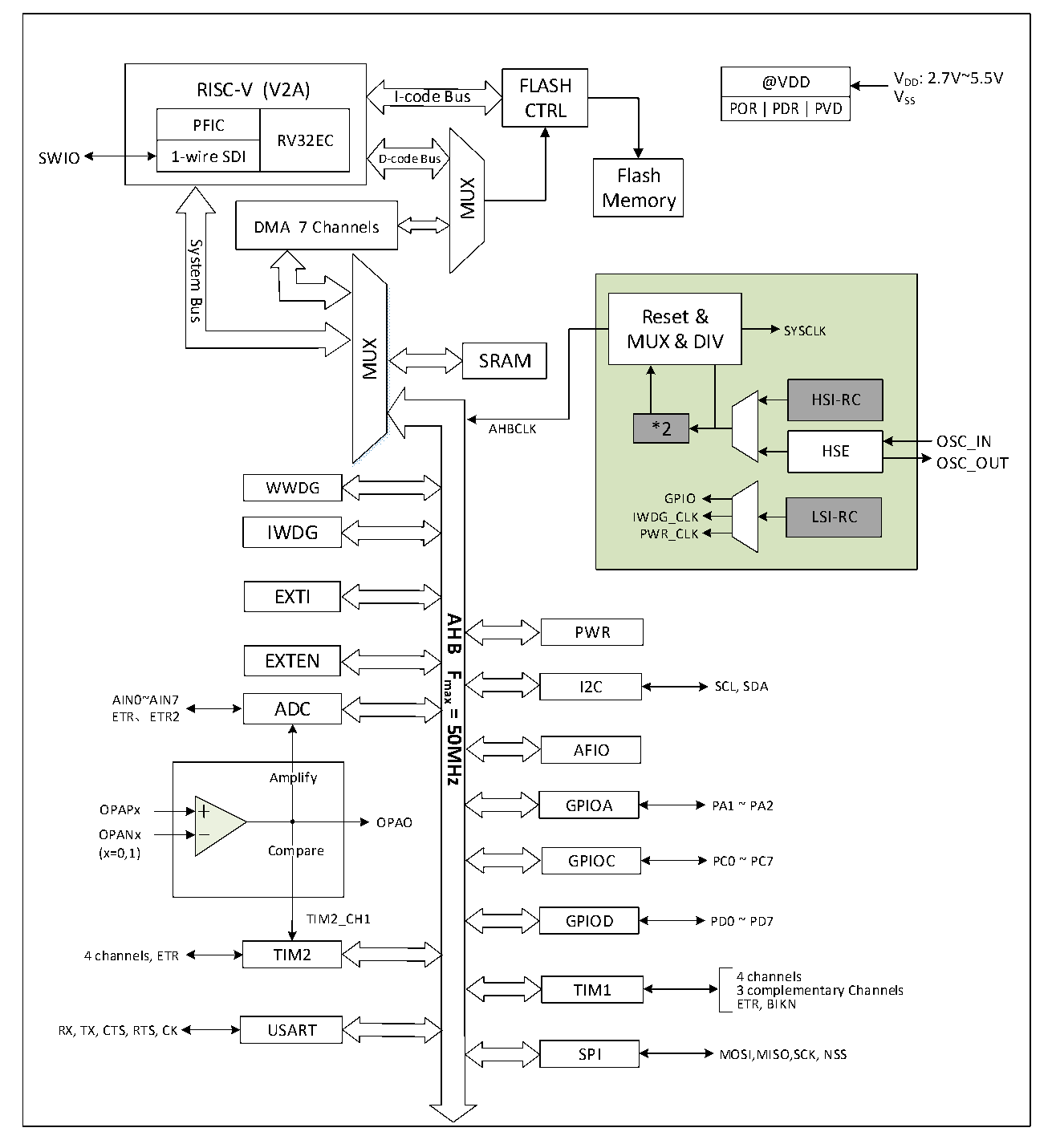
CH32V003
EVT examples
63 routines in EVT/EXAM:
ADC 7 · APPLICATION 1 · DMA 2 · EXTI 1 · FLASH 2 · GPIO 1 · I2C 6 · IAP 1 · INT 2 · IWDG 1 · OPA 1 · PWR 4 · RCC 2 · SDI_Printf 1 · SPI 5 · SYSTICK 1 · TIM 16 · USART 8 · WWDG 1
Documents
| Document | Kind | English | 中文 |
|---|---|---|---|
| CH32V003DS0.PDF | datasheet | page mirror v1.8 | page mirror v1.8 |
| CH32V003RM.PDF | reference-manual | page mirror v1.9 | page mirror v1.9 |
| CH32V003EVT.ZIP | evt | - | page mirror v1.0 |
Evaluation boards
- board-manual:en: CH32V00x Evaluation Board Reference-EN.pdf
- board-manual:zh: CH32V00x评估板说明书.pdf
- schematic-pdf: CH32V00xSCH.pdf
1 board schematics under EVT/PUB/SCHPCB/: CH32V003F4P6-R0
Reference
Address map
| Region | Base | Kind |
|---|---|---|
| APB1PERIPH | 0x40000000 |
bus |
| PERIPH | 0x40000000 |
bus |
| APB2PERIPH | 0x40010000 |
bus |
| AHBPERIPH | 0x40020000 |
bus |
| FLASH | 0x00000000 |
link-origin |
| RAM | 0x20000000 |
link-origin |
| FLASH | 0x08000000 |
memory |
| OB | 0x1ffff800 |
memory |
| SRAM | 0x20000000 |
memory |
link-origin is what the EVT linker scripts use; the memory row for FLASH is the address the device header states. Both windows are real – CH32V307 answers at 0x08000000 and at 0x00000000.
Peripheral base addresses are in memory_map.csv; interrupt numbers in interrupts.csv.
Data: ch32-device-data (evidence/ and index/ – each value carries its evidence and confidence there).